
Publications
- A. M. Shen, C.-L. Chen, K. Kim, B. Cho, A. Tudor, and Y. Chen, Analog Neuromorphic Module Based on Carbon Nanotube Synapses, ACS Nano, 6117-6122 (2013)
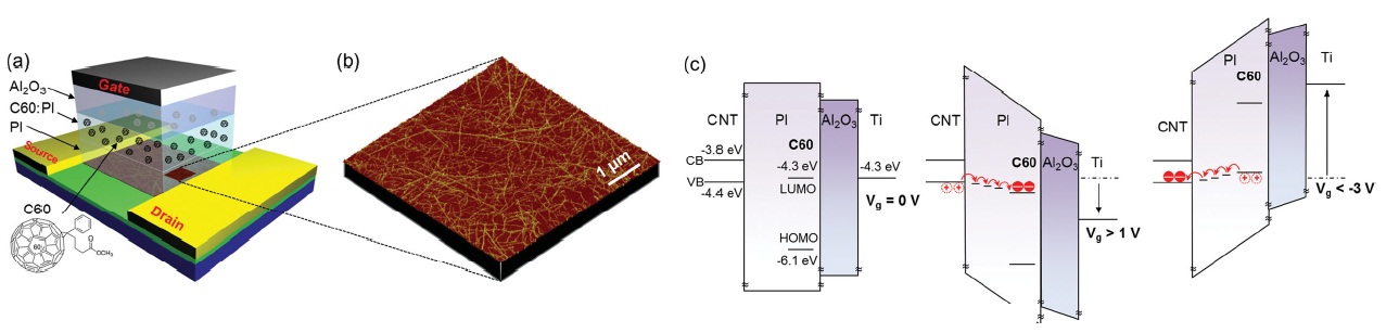
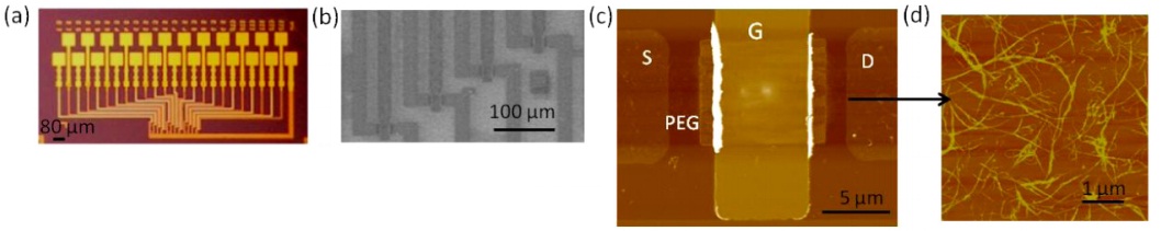
- B. Cho , K. Kim , C.-L. Chen , A.M. Shen , Q. Truong, and Y. Chen, Nonvolatile Analog Memory Transistor Based on Carbon Nanotubes and C60 Molecules, Small, 1-5(2013)
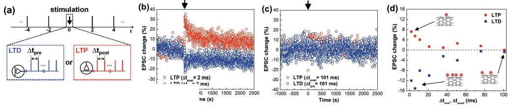
- K. Kim , C.-L. Chen , Q. Truong, A.M. Shen, and Y. Chen, A Carbon Nanotube Synapse with Dynamic Logic and Learning, Advanced Materials, 1693-1698, (2013)
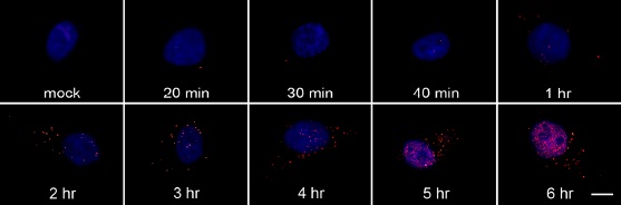
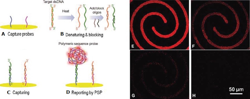
- S. Huang, C. Yu, G. Cheng, and Y. Chen, Detection of Single Influenza Viral RNA in Cells Using a Polymeric Sequence Probe Analytical Chemistry(2012)
- T. Lee, and Y. Chen, Organic resistive nonvolatile memory materials, MRSBulletin, 37(2) 144-149, (2012)
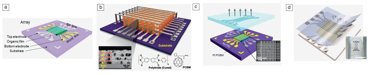
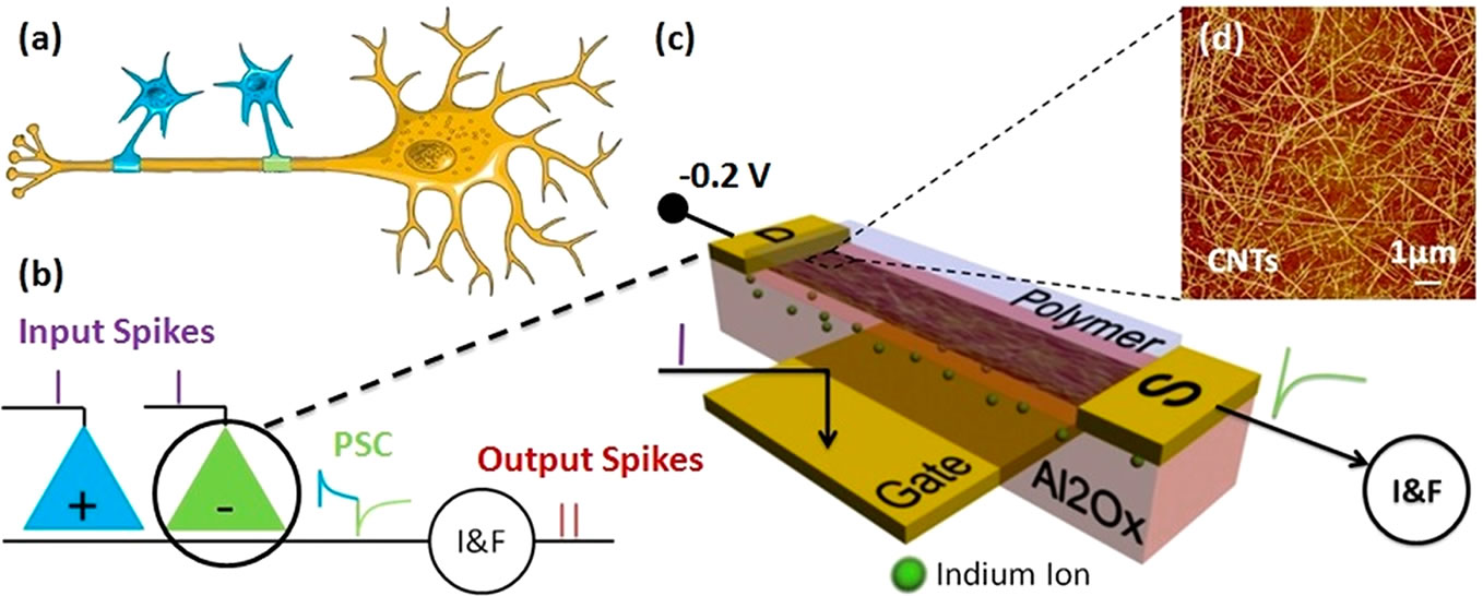
- C-L Chen, K. Kim, Q.Truong, A Shen, and Y. Chen, A Spiking Neuron Circuit Based on Acarbon Nanotube Transistor, Nanotechnology, 23(27), 1-6, (2012)
- S. Huang and Y. Chen, Polymeric Sequence Probe for Single DNA Detection, Analytical Chemistry, 83 (19), 7250-7254, (2011)
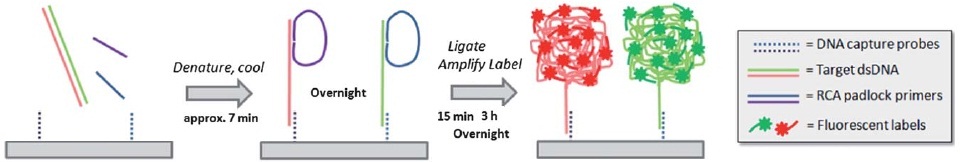
- E. Schopf, Y. Liu, J. C. Deng, S. Yang, G. Chengb, and Y. Chen, Mycobacterium Tuberculosis Detection Via Rolling Circle Amplification, Analytical Methods, 3, 267-273, (2011)
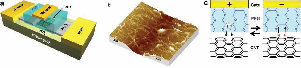
- Y. S. Ahn, K. Kim, H. K. Park, H. T. Hahn, and Y. Chen, Functionalized Carbon Nanotube Networks with Field-Tunable Bandgaps, Advanced Materials, 23, 3075-3079, (2011)
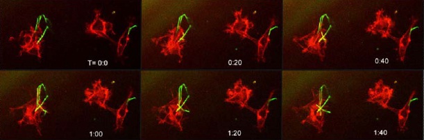
- Y. Lei, S. Huang, P. Sharif-Kashani, Y. Chen, P. Kavehpour, $ T.Segura, Incorporation of active DNA/cationic polymer polyplexes into hydrogel scaffolds, Biomaterials,,34, 9106-16, 2010
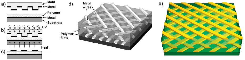
- C. Stuart, H.-K. Park, and Y. Chen, Fabrication of a 3D Nanoscale Crossbar Circuit by Nanotransfer-Printing Lithography, Small, 6, 1663-1668 (2010)
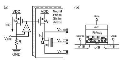
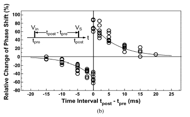
- L. Zhang, Q. Lai, and Y. Chen, Configurable Neural Phase Shifter With Spike-Timing-Dependent Plasticity, IEEE Electron Device Letters, 31, 716-718 (2010)
- E. Schopf, and Y. Chen, Attomole DNA Detection Assay via Rolling Circle Amplification and Single Molecule Detection, Analytical Biochemistry, 397, 115-117 (2010)
- Q. Lai, L. Zhang, W.F. Stickle, R.S. Williams, and Y. Chen, Ionic/electronic Hybrid Materials Integrated in a Synaptic Transistor with Signal Processing and Learning Functions, Advanced Materials, 22, 1-6 (2010)
- K. Galatsis, K.L. Wang, M. Ozkan, C.S. Ozkan, Y. Huang, J.P. Chang, H.G. Monbouquette, Y. Chen, P. Nealey, and Y. Botros, Patterning and Templating for Nanoelectronics, Advanced Materials, 22, 769-778 (2009)
- Y.R. Ahn, Y. Chen, and H.T. Hahn, A Resist for Electric Imprint Lithography, Microelectronic Engineering, 86, 392-396, (2009)
- Qiaxi, L., Lei, L., Zhiyong, L., Stickle, W.F., Williams, R.S., Chen, Y., Analog Memory Capacitor Based on Field-Configurable Ion-Doped Polymers, Applied Physics Letters 95, 213503, (2009)
- Y. Chang, S. Huang and Y. Chen, Biomolecular Nanopatterning by Electrophoretic Printing Lithography, Small, 5, 63 (2009)
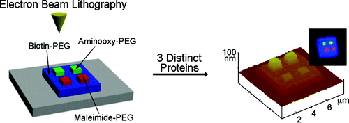
- K. Christman, E. Schopf, R. Broyer, R. Li, Y. Chen, and H. Maynard, Nanoscale Assembly of Multilayer Multicomponent Protein Patterns by Electron Beam Lithography, Journal of the American chemical Society, 131, 521-527 (2009)
- Z. Gu, S. Huang and Y. Chen, Biomolecular Nanopatterning by Magnetic Electric Lithography, Angewandte Chemie International Edition, 121, 970 (2009)
- P. Parthasarathy, P.M. Mendes, E. Schopf, J.A. Preece, J.F. Stoddart and Y. Chen, Spatially Controlled Assembly of Nanomaterials at the Nanoscale, Journal of Nanoscience and Nanotechnology, 9, 650, (2009)
- J. Bai, S. Huang, L. Wang, Y. Chen and Y. Huang, Fluid assisted assembly of nanoparticle array inside of inorganic nanotubes, Journal of Materials Chemistry, 19, 921 (2008)
- K. Christman, V. Vazquez-Dorbatt, E. Schopf, C. Kolodziej, R. Li, R. Broyer, Y. Chen and H. Maynard, Nanoscale Patterns of VEGF and bFGF Using Electron Beam Lithography and a Heparin Mimicking Polymer, Journal of the American Chemical Society, 130, 16585, (2008)
- E. Schopf, N.O. Fischer, Y. Chen and J.B.-H. Tok, Sensitive and Selective Viral DNA Detection Assay via Microbead-Based Rolling Circle Amplification, Bioorganic & Medicinal Chemistry Letters, 18, 587-5874 (2008)
- Q.X. Lai, Z.Y. Li, L. Zhang, X.M. Li, W.F. Stickle, Z.H. Zhu, Z. Gu, T.I. Kamins, R.S. Williams and Y. Chen, An Organic/Si Nanowire Hybrid Field Configurable Transistor, Nano Letters, 8, 876-880 (2008)
- S. Huang and Y. Chen, Ultrasensitive Fluorescence Detection of Single Protein Molecules Manipulated Electrically on Au Nanowire, Nano Letters, 8, 2829-2833 (2008)
- H.X. Ge, W.J. Shen and Y. Chen, Electrically Curable Double-Layer Polymer Resist for Dynamic Nanoscale Lithography, Soft Matter, 4, 1178-1182 (2008)
- A.O. Fung, V. Kapadia, E. Pierstorff, D. Ho and Y. Chen, Induction of Cell Death by Magnetic Actuation of Nickel Nanowires Internalized by Fibroblasts, The Journal of Physical Chemistry. C , 112, 15085-15088 (2008)
- D.S. Choi, J. Park, S. Kim, D.H. Gracias, M.K. Cho, Y.K. Kim, A. Fung, S.E. Lee, Y. Chen, S. Khanal, S. Baral, and J.-H. Kim, Hyperthermia with Magnetic Nanowires for Inactivating Living Cells, Journal of Nanoscience and Nanotechnology, 8, 1-5, (2008)
- P.M. Mendes, K.L. Christman, P. Parthasarathy, E. Schopf, J. Ouyang, Y. Yang, J.A. Preece, H.D. Maynard, Y. Chen and J.F. Stoddart, Electrochemically Controllable Conjugation of Proteins on Surfaces, Bioconjugate Chemistry, 18, 1919-1923, (2007)
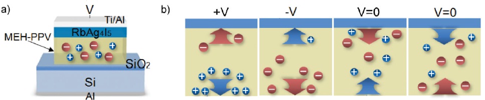
- X.F. Liang, Y. Chen, L. Shi, J. Lin, J. Yin and Z.G. Liu, Resistive Switching and Memory Effects of AgI Thin Film. Journal of Physics D-Applied Physics, 40, 4767-4770, (2007)
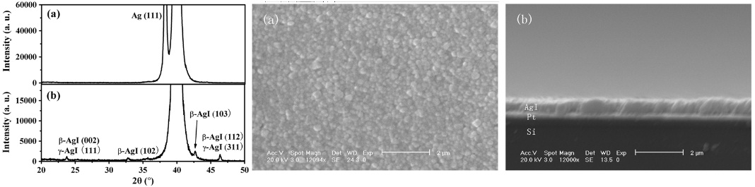
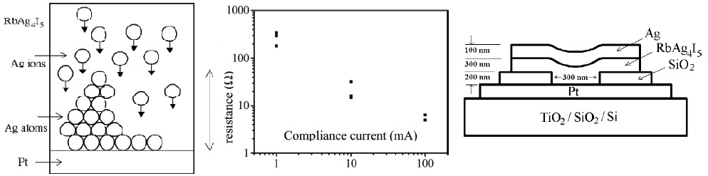
- X.F. Liang, Y. Chen, L. Chen, J. Yin and Z.G. Liu, Electric Switching and Memory Devices Made From RbAg4I5 Films, Applied Physics Letters, 90, 022508-022510, (2007)
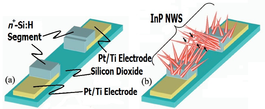
- N.P. Kobayashi, V.J. Logeeswaran, M. Saif Islam, X.M. Li, J. Straznicky, S.Y. Wang, R.S. Williams and Y. Chen, Hydrogenated Microcrystalline Silicon Electrodes Connected by Indium Phosphide Nanowires, Applied Physics Letters, 91, 113116, (2007)
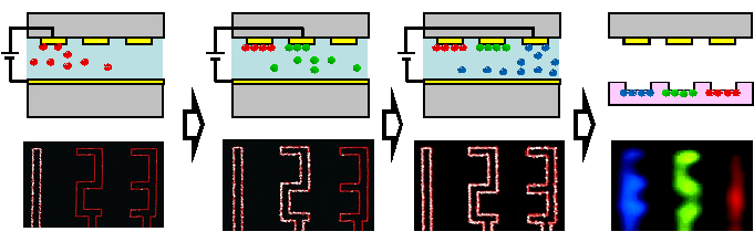
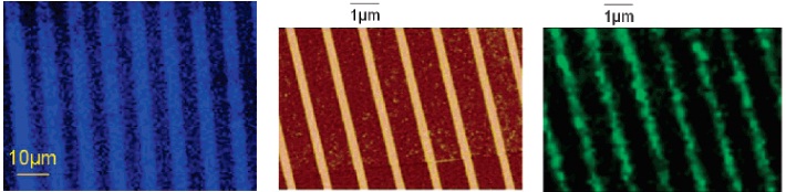
- S. Huang, E. Schopf and Y. Chen, Dynamically Configurable Biomolecular Nanoarrays, Nano Letters, 7, 3116-3121, (2007)
- D. Choi, A. Fung, H. Moon, D. Ho, Y. Chen, E. Kan, Y. Rheem, B. Yoo and N. Myung, Transport of Living Cells with Magnetically Assembled Nanowires, Biomedical Microdevices, 9, 143-148, (2007)
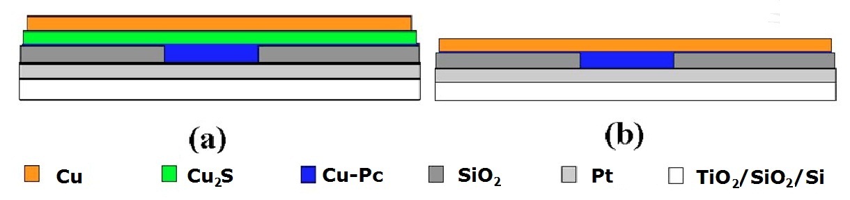
- L. Chen, Y.D. Xia, X.F. Liang, K.B. Yin, J. Yin, Z.G. Liu and Y. Chen, Nonvolatile Memory Devices with Cu2S and Cu-Pc Bilayered Films, Applied Physics Letters, 91, 073511-073513, (2007)
- Y. Chang, Y.S. Ahn, H.T. Hahn and Y. Chen, Sub-Micrometer Patterning of Proteins by Electric Lithography, Langmuir, 23, 4112-4114, (2007)
- C. Stuart, Q.F. Xu, R.J. Tseng, Y. Yang, H.T. Hahn, Y. Chen, W. Wu & R.S. Williams, Nanofabrication Module Integrated with Optical Aligner, Journal of Vacuum Science & Technology B 24, 539-542, (2006)
- S. Patil, Q.X. Lai, F. Marchioni, M.Y. Jung, Z.H. Zhu, Y. Chen and F. Wudl, Dopant-Configurable Polymeric Materials for Electrically Switchable Devices, Journal of Materials Chemistry 16, 4160-4164, (2006)
- Q.X. Lai, Z.H. Zhu, Y. Chen, S. Patil and F. Wudl, Organic Nonvolatile Memory by Dopant-Configurable Polymer, Applied Physics Letters88, 133515, (2006))
- T. Hogg, Y. Chen and P.J. Kuekes, Assembling Nanoscale Circuits with Randomized Connections, Ieee Transactions on Nanotechnology 5, 110-122, (2006)
- W. Shen, Y. Chen & Q. Pei, Electric Lithography by Electrochemical Polymerization, Applied Physics Letters, 87, 124106 (2005)
- G.-Y. Jung, Z. Li, W. Wu, Y. Chen, D.L. Olynick, S.-Y. Wang, W.M. Tong, and R.S. Williams, Vapor-Phase Self-Assembled Monolayer for Improved Mold Release in Nanoimprint Lithography, Langmuir, 21, 1158-1161, (2005)
- Z. Li, Y. Chen, X. Li, T.I. Kamins, K. Nauka, and R.S. Williams, Sequence-Specific Label-Free DNA Sensors Based on Silicon Nanowires, Nano Letters, 4(2), 245-247, (2004)
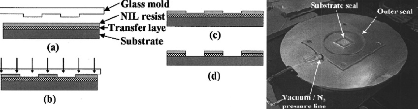
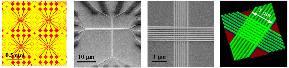
- G.Y. Jung, S. Ganapathiappan, D.A.A. Ohlberg, D.L. Olynick, Y. Chen, W.M. Tong, and R. S. Williams, Fabrication of a 34x34 Crossbar Structure at 50 nm Half-Pitch by UV-based Nanoimprint Lithography, Nano Letters, 4(7), 1225-1229, (2004)
- G.-Y. Jung, S. Ganapathiappan, X Li, D.A.A. Ohlberg, L.D. lynick, Y. Chen, W. Wu, S.-Y. Wang, W.M. Tong, and R.S. Williams, Fabrication Process of Molecular Memory Circuits by Nanoimprint Lithography, SPIE, 5374, 197-202, (2004)
- Y. Chen, D.A.A. Ohlberg, X. Li, D. Stewart, and R.S. Williams, Nanoscale Molecular-Switch Devices Fabricated by Imprint Lithography, Appl. Phys. Lett., 82, 1610-1612,(2003))
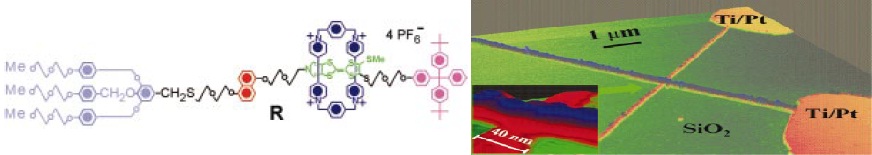
- Y. Chen, G. Jung, D.A.A. Ohlberg, X. Li, D. Stewart, J. O., Jeppesen, Nielsen, J.F., Stoddart, and R.S. Williams, Nanoscale Molecular-Switch Crossbar Circuits, Nanotechnology, 14, 462-468,(2003)
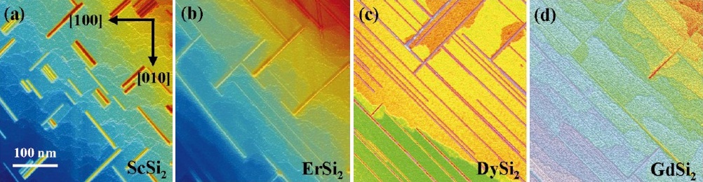
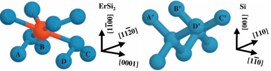
- Y. Chen, D.A.A. Ohlberg, G. Medeiros-Ribeiro, Y.A. Chang, and R.S. Williams, Growth and Evolution of Epitaxial Erbium Disilicides Nanowires on Si(001), Appl. Phys., A71, 1-6, (2002)
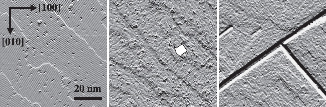
- Y. Chen, D.A.A. Ohlberg, and R.S. Williams, Nanowires of Four Epitaxial Hexagonal Silicides Grown on Si(001), Appl. Phys., 91, 3213-3218,(2002)
- C.M. Pelto, Y.A. Chang, Y. Chen, and R.S. Williams, Issues Concerning the Preparation of Ohmic Contacts to n-GaN, Solid State Elec., 45, 1597-1600, (2001)
- T.I. Kamins, R.S. Williams, Y. Chen, Y.L. Chang, and Y.A. Chang, Chemical Vapor Deposition of Si Nanowires Nucleated by TiSi2 Islands on Si, Appl. Phys. Lett., 76, 562-564,(2000)
- Y. Chen, D.A.A. Ohlberg, G. Medeiros-Ribeiro, Y.A. Chang, and R.S. Williams, Self-Assembled Growth of Epitaxial Erbium Disilicide Nanowires on Silicon(001), Appl. Phys. Lett., 76, 4004-4006, (2000)
- D.B. Ingerly, Y. Chen, R.S. William, T. Takeuchi, and Y.A. Chang, Low Resistance Ohmic Contacts to n-GaN and n-AlGaN Using NiAl, Appl. Phys. Lett., 77, 382-384, (2000)
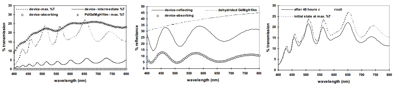
- R. Armitage, M. Rubin, T. Richardson, N. O'Brien, and Y. Chen, Solid-State Gadolinium-Magnesium Hydride Optical Switch, Appl. Phys. Lett., 75, 1863-1865, (1999)
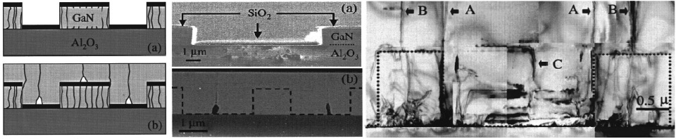
- Y. Chen, R. Schneider, Y.S Wang, R.S. Kern, C.H. Chen, and C.P. Kuo, Dislocation Reduction in GaN Thin Films via Lateral Overgrowth From Trenches, Appl. Phys. Lett., 75, 2062-2064, (1999)
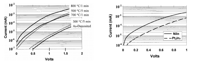
- D.B. Ingerly, Y.A. Chang, and Y. Chen,The Electrical Behavior of Pt3In7 and NiIn Contacts to p-GaN, Appl. Phys. Lett., 74, 2480-2482, (1999)
- A. Vertikov, M. Kuball, A.V. Nurmikko, Y. Chen, and S.Y. Wang, Near-field Optical Study of InGaN/GaN Epitaxial Layers and Quantum Wells, Appl. Phys. Lett., 72, 2645-2647, (1998)
- Y. Chen, T. Takeuchi, H. Amano, I. Akasaki, N. Yamada, Y. Kaneko, and S.Y. Wang, Pit Formation in GaInN Quantum Wells, Appl. Phys. Lett., 72, 710-712, (1998)
- Z. Liliental-Weber, Y. Chen, S. Ruvimov, and J. Washburn, Formation Mechanism of Nanotubes in GaN, Phys. Rev. Lett., 79, 2835-2838, (1997)
- Y. Chen, and J. Washburn, Structural Transition in Large Lattice-Mismatch Heteroepitaxy, Phys. Rev. Lett., 77, 4046-4649, (1997)
- Z. Liliental-Weber, C. Kisielowski, S. Ruvimov, Y. Chen, and J. Washburn, Structural Characterization of Bulk GaN Crystals Grown Under High Hydrostatic Pressure, J. Electron. Mater., 25, 1545-1547,(1996)
- X. Jin, Y. Chen, X.M. Lin, D.S. Dong, Y. Chen, M. Xu, W.R. Zhu, X. Wang, X.L. Shen, and L. Li,Interface Structure of FCC Mn on GaAs(001), Appl. Phys. Lett., 70, 2455-2457,(1996)
- Y. Chen, X.W. Lin, Z. Liliental-Weber, J. Washburn, J.F. Klem, and J.Y. Tsao, Dislocation Formation Mechanism in Strained InGaAs Islands, Appl. Phys. Lett., 68, 111-113,(1996)
- J. Jasinski, Y. Chen, J. Washburn, Z. Liliental-Weber, H.H., Tan, C., Jagadish, and M. Kaminska, Recrystallization of High Energy As Implanted GaAs Studeied by TEM, Appl. Phys. Lett., 68, 1273-1275,(1996)
- Y. Chen, Z. Liliental-Weber, J. Washburn, J.F. Klem, and J.Y. Tsao, Nucleation of Misfit Dislocations in InGaAs Epilayers Grown on GaAs Substrates, Appl. Phys. Lett., 66, 499-501, (1995)
- Y. Chen, X. Liu, E. Weber, E.D. Bourret, Z. Liliental-Weber, E.E., Haller, J. Washburn, J.D. Olego, D.R. Dorman, J.M. Gaines, and N.R. Tasker, Structures and Electronic Properties of Misfit Dislocations in ZnSe/GaAs(001) Heterojunctions, Appl. Phys. Lett., 65, 549-551, (1994)
- N.D. Zakharov, P. Werner, Y. Chen, W. Swider, Z. Liliental-Weber, J. Washburn, J.F. Klem, and J.Y. Tsao, Compositional Nonuniformities and Strain Relaxation at Misoriented InGaAs/GaAs Interfaces, J. Electron. Mater. 22, 1341-1343, (1993)
- Z. Liliental-Weber, Y. Chen, P. Werner, N.D. Zakharov, W. Swider, J. Washburn, J.F. Klem, and J.Y. Tsao, Interfacial Defects and Morphology of InGaAs Epilayers Grown on Tilted GaAs Substrates, J. Vac. Sci. Technol. B11, 1379-1382, (1993)
- Y. Chen, Z. Liliental-Weber, J. Washburn, J.F. Klem, and J.Y. Tsao, Nonconservative Formation of < 100> Misfit Dislocation Arrays at InGaAs/GaAs(001) Interfaces During Post-Growth Annealing, Appl. Phys. Lett., 63, 2234-2236, (1993)
- P. Werner, N.D. Zakharov, Y. Chen, Z. Liliental-Weber, J. Washburn, J.F. Klem, and J.Y. Tsao, Stress Releasing Mechanisms in InGaAs Layers Grown on Misoriented GaAs() Substrate, Appl. Phys. Lett., 62, 2798-2800, (1993)
- Y. Chen, N.D. Zakharov, P. Werner, Z. Lilental-Weber, J. Washburn, J.F. Klem, and J.Y. Tsao, Structure and Location of Misfit Dislocations in InGaAs Epilayers Grown on Vicinal GaAs(001) Substrates, Appl. Phys. Lett., 62, 1536-1538, (1993)
- Z. Liu, Y. Chen, and X.Z. Wen, Characterization of the Oxide Film on Molybdenum Surface, Surface Sci., 208, L15-L20,(1989)
- X. Zhou, L.Z. Liu, Y. Zhu, G. Chen, Y. Chen, Q. Zhang, and W. Guan, Experimental Verification of Superconducting Phase Seperation Model in ZrCo Metallic Glass, Solid State Commun, 69, 981 (1989)
- Y. Chen, Z.G. Liu, and D. Feng, Atom Probe Microanalysis of an Elivar Type Alloy, Scripta. Met., 22, 1075, (1988)
- Z.G. Liu, Y. Chen, and D. Feng, The Decomposition of an Elinvar Alloy, Z.Metallkunde, 79, 643, (1988)